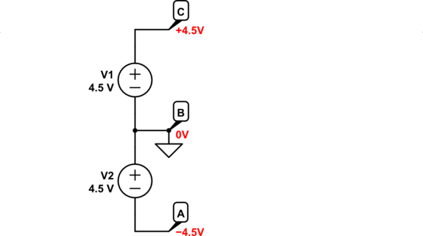
This is a copy of your own design, with labels to show potentials everywhere, and drawn in a way that makes it easier to see what's going on:

simulate this circuit – Schematic created using CircuitLab
On the left I used the ground symbol to declare that in all my algebra, node A has potential 0V. Every other node's potential will be quoted with respect to this "ground" potential. Clearly the voltage source V1 ensures that node C's potential is 9V higher than node A:
$$ V_C = V_A + V_1 = 0{\rm V} + 9{\rm V} = +9{\rm V} $$
The resistors divide the total potential difference between each end by 2. That total is \$V_C - V_A = V_1 = 9{\rm V}\$, so each resistor will have half of that, \$V_{R1}=V_{R2}=4.5V\$, across it. Therefore:
$$ V_B = V_A + V_{R2} = 0{\rm V} + \frac{1}{2}V_1 = 0{\rm V} + 4.5{\rm V} = +4.5{\rm V} $$
Alternatively, you could say that node B is 4.5V lower in potential that node C, giving the same result:
$$ V_B = V_C - V_{R1} = +9{\rm V} - \frac{1}{2}V_1 = +9{\rm V} - 4.5{\rm V} = +4.5{\rm V} $$
On the right, I've moved the ground symbol. All that does is say "node B has zero volts". It doesn't change the behaviour of the circuit at all, it's just an arbitrary "reference point", a "zero" for all the algebra. Consequently I've had to alter some "absolute" values to reflect that change, but R1 still has 4.5V across it, as does R2, and we can make the same statements - node A is 4.5V less than node B, and node C is 4.5V greater than B, regardless of where I put my ground symbol.
That is why the circuit on the right represents your desired state of affairs, a "fake ground", an abitrary 0V half way between the potentials of the battery terminals, whatever they may be. But you also need to shift all the potentials, to -4.5V, +4.5V and 0V, to reflect this new voltage labelling and referencing regime. Nothing's changed in terms of behaviour and functionality, just the labels.
Sadly, this new ground has issues - it's not the same as this:
simulate this circuit
If you did this (use two 4.5V batteries), all your problems instantly go away, there's no way A or C can be anything but 4.5V different from B (assuming the batteries are matched and fully charged).
When using a resistor divider, though, the convenient 4.5V across resistors R1 and R2 will change as a result of any amount of current flowing through them, so that 0V won't stay "0V" under any appreciable load. Rather, from a more correct perspective, since you are declaring \$V_B=0{\rm V}\$, you can say that's always true, but then strictly speaking it would be \$V_A\$ and \$V_C\$ that are changing, relative to \$V_B\$, as a result of changing potential differences across R1 and R2.
That's a problem largely solved (with some caveats I won't talk about here) by an op-amp voltage follower:

simulate this circuit
The op-amp becomes responsible for sinking and sourcing any current requirement (shown in blue) at its output directly to/from the supply rails, bypassing R1 and R2 altogether. Therefore those resistors always have 4.5V across them, and the op-amp always duplicates their now-always-correct "0V" junction potential at its own output. We would say that this is a "low-impedance source" of 0V.
Also, you can raise the values of R1 and R2, and still maintain a good clean and stable "0V" at their junction, for reduced power wastage in those resistors.
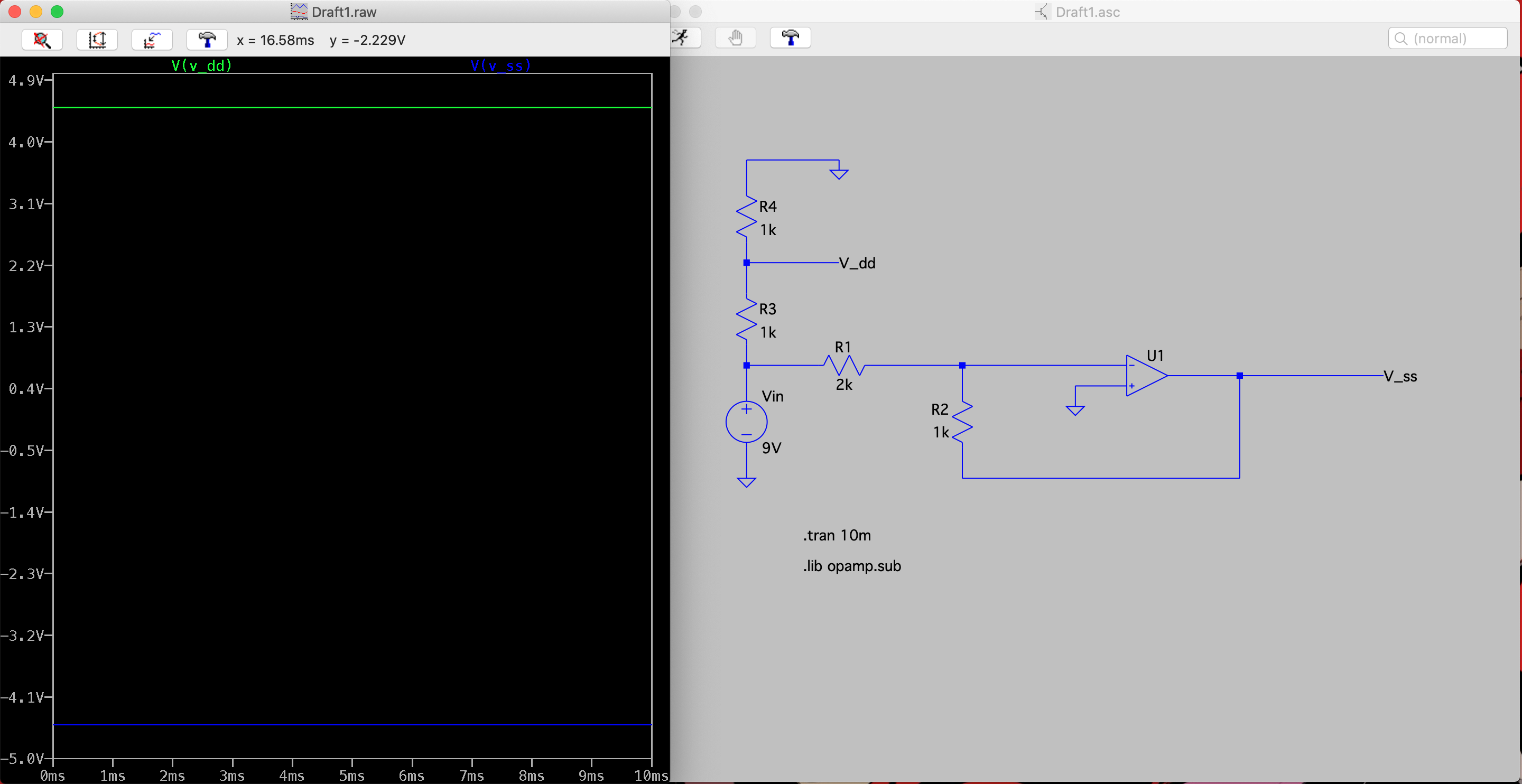
Ironically, all this is moot, because the amplifier design has most of the elements necessary to overcome this lack of "centre-ground" already. There's only one additional resistor necessary to make the circuit operate as you want, R6 here:

simulate this circuit
Capacitors C3, C4 and C5 isolate all AC fluctuations from any mean DC offsets (shown in red, also called "quiescent" levels, or "DC operating point", or "biasing") of the op-amps's inputs and output. Such "biasing" is established by the resistor divider R5 & R6, to a DC potential half-way between the 0V and +9V supply rails. This fools the op-amp into "thinking" that all its signals fluctuate around +4.5V, smack in the middle of its own supply potentials, when in reality \$V_{IN}\$ and \$V_{OUT}\$ are actually wobbling around 0V.
Just one extra resistor, R6, no need for a fake ground, or another op-amp to strengthen it.